- 您现在的位置:买卖IC网 > Sheet目录286 > 24FC515T-I/SM (Microchip Technology)IC EEPROM 512KBIT 1MHZ 8SOIC
�� �
�
�24AA515/24LC515/24FC515�
�2.0�
�PIN� DESCRIPTIONS�
�2.4�
�Serial� Clock� (SCL)�
�The� descriptions� of� the� pins� are� listed� in� Table� 2-1.�
�This� input� is� used� to� synchronize� the� data� transfer� from�
�and� to� the� device.�
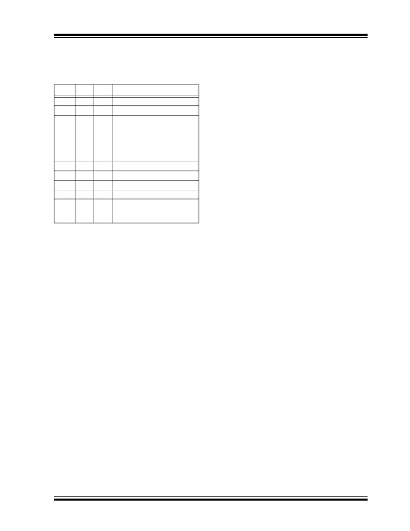
�TABLE� 2-1:�
�PIN� FUNCTION� TABLE�
�Name� PDIP� SOIJ�
�Function�
�2.5�
�Write-Protect� (WP)�
�A0�
�A1�
�A2�
�1�
�2�
�3�
�1�
�2�
�3�
�User� Configurable� Chip� Select�
�User� Configurable� Chip� Select�
�Non-Configurable� Chip� Select.�
�This� pin� must� be� connected� to� either� V� SS� or� V� CC� .� If� tied�
�to� V� SS� ,� write� operations� are� enabled.� If� tied� to� V� CC� ,�
�write� operations� are� inhibited� but� read� operations� are�
�not� affected.�
�This� pin� must� be� hard� wired� to�
�logical� 1� state� (V� CC� ).� Device�
�will� not� operate� with� this� pin�
�3.0�
�FUNCTIONAL� DESCRIPTION�
�left� floating� or� held� to� logical� 0�
�(V� SS� ).�
�The� 24XX515� supports� a� bidirectional� 2-wire� bus� and�
�data� transmission� protocol.� A� device� that� sends� data�
�V� SS�
�SDA�
�SCL�
�WP�
�V� CC�
�4�
�5�
�6�
�7�
�8�
�4�
�5�
�6�
�7�
�8�
�Ground�
�Serial� Data�
�Serial� Clock�
�Write-Protect� Input�
�+1.7� to� 5.5V� (24AA515)�
�onto� the� bus� is� defined� as� a� transmitter,� and� a� device�
�receiving� data� as� a� receiver.� The� bus� must� be�
�controlled� by� a� master� device� which� generates� the�
�Serial� Clock� (SCL),� controls� the� bus� access,� and�
�generates� the� Start� and� Stop� conditions� while� the�
�24XX515� works� as� a� slave.� Both� master� and� slave� can�
�+2.5� to� 5.5V� (24LC515)�
�+2.5� to� 5.5V� (24FC515)�
�operate� as� a� transmitter� or� receiver,� but� the� master�
�device� determines� which� mode� is� activated.�
�2.1�
�A0,� A1� Chip� Address� Inputs�
�The� A0,� A1� inputs� are� used� by� the� 24XX515� for� multiple�
�device� operations.� The� levels� on� these� inputs� are�
�compared� with� the� corresponding� bits� in� the� slave�
�address.� The� chip� is� selected� if� the� compare� is� true.�
�Up� to� four� devices� may� be� connected� to� the� same� bus�
�by� using� different� Chip� Select� bit� combinations.� In� most�
�applications,� the� chip� address� inputs� A0� and� A1� are�
�hard-wired� to� logic� ‘� 0� ’� or� logic� ‘� 1� ’.� For� applications� in�
�which� these� pins� are� controlled� by� a� microcontroller� or�
�other� programmable� device,� the� chip� address� pins�
�must� be� driven� to� logic� ‘� 0� ’� or� logic� ‘� 1� ’� before� normal�
�device� operation� can� proceed.�
�2.2�
�A2� Chip� Address� Input�
�The� A2� input� is� non-configurable� Chip� Select.� This� pin�
�must� be� tied� to� V� CC� in� order� for� this� device� to� operate.�
�2.3�
�Serial� Data� (SDA)�
�This� is� a� bidirectional� pin� used� to� transfer� addresses�
�and� data� into� and� data� out� of� the� device.� It� is� an� open-�
�drain� terminal,� therefore,� the� SDA� bus� requires� a� pull-�
�up� resistor� to� V� CC� (typical� 10� k� Ω� for� 100� kHz,� 2� k� Ω� for�
�400� kHz� and� 1� MHz).�
�For� normal� data� transfer� SDA� is� allowed� to� change� only�
�during� SCL� low.� Changes� during� SCL� high� are�
�reserved� for� indicating� the� Start� and� Stop� conditions.�
�?� 2008� Microchip� Technology� Inc.�
�DS21673G-page� 5�
�发布紧急采购,3分钟左右您将得到回复。
相关PDF资料
24FC64T-I/MF
IC EEPROM 64KBIT 1MHZ 8DFN
24LC014H-I/P
IC EEPROM 1KBIT 400KHZ 8DIP
24LC014T-E/OT
IC EEPROM 1KBIT 400KHZ SOT23-6
24LC01B-I/SNG
IC EEPROM 1KBIT 400KHZ 8SOIC
24LC024H-I/ST
IC EEPROM 2KBIT 400KHZ 8TSSOP
24LC025T-E/MC
IC EEPROM 2KBIT 400KHZ 8DFN
24LC04B-E/P
IC EEPROM 4KBIT 400KHZ 8DIP
24LC04BH-E/P
IC EEPROM 4KBIT 400KHZ 8DIP
相关代理商/技术参数
24FC64
制造商:MICROCHIP 制造商全称:Microchip Technology 功能描述:64K I2C? Serial EEPROM
24FC64-E/CS16K
制造商:MICROCHIP 制造商全称:Microchip Technology 功能描述:64K I2C? Serial EEPROM
24FC64-E/MC
制造商:MICROCHIP 制造商全称:Microchip Technology 功能描述:64K I2C? Serial EEPROM
24FC64-E/MNY
制造商:MICROCHIP 制造商全称:Microchip Technology 功能描述:64K I2C? Serial EEPROM
24FC64-E/MS
制造商:MICROCHIP 制造商全称:Microchip Technology 功能描述:64K I2C? Serial EEPROM
24FC64-E/OT
制造商:MICROCHIP 制造商全称:Microchip Technology 功能描述:64K I2C? Serial EEPROM
24FC64-E/P
制造商:MICROCHIP 制造商全称:Microchip Technology 功能描述:64K I2C? Serial EEPROM
24FC64-E/SM
制造商:MICROCHIP 制造商全称:Microchip Technology 功能描述:64K I2C? Serial EEPROM